



Optimize Stencil Design for SMT Circuit Boards
The stencil is a critical component in surface mount technology assembly (SMT), enabling the accurate and consistent deposition of solder paste onto PCB pads. It plays a major role in determining the quality and reliability of finished electronic products, and its performance can be dramatically improved by regular inspection, cleaning and maintenance. This comprehensive guide explores the types, materials, design considerations and best practices of smt circuit board stencils to help manufacturers optimize their performance.
Stencil design is a crucial process that determines the volume, uniformity and definition of material deposits on a substrate. In order to achieve these goals, it is important to have a precise relationship between the pad size, the aperture opening and the stencil foil thickness. Using parameters such as area ratio (the area beneath the aperture opening divided by the inside of the aperture wall) and aspect ratio (aperture width divided by stencil thickness) helps ensure that the correct amount of solder paste is deposited on the pads of the circuit board.
Using a stencil that is too thick or too small for the aperture opening can lead to problems such as bridging and solder balls. Ideally, the aperture opening should be marginally smaller than the pad size to ensure that the deposited solder paste will adhere to the pads without sticking to the walls of the aperture.
The design of the stencil is also critical to proper paste transfer and printing. Aspect ratios, area ratios and other geometric dimensions must be carefully matched to the specific application. Stencil material is often stainless steel or nickel, but other high-performance materials may be employed to meet the printing requirements of a particular application.
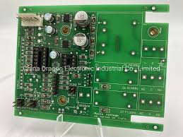
How to Optimize Stencil Design for SMT Circuit Boards
Once the stencil has been designed, it must undergo a rigorous fabrication and cleaning process to eliminate any contaminants or residues that could interfere with optimum paste release during the printing process. In addition, the stencil must be inspected and cleaned after each use to prevent blockages from developing.
The SMT assembly process imposes very high standards on processing plants, demanding the highest levels of quality and consistency. As a result, a stencil is a key component in the success of SMT assemblies, and the right one can significantly improve production efficiency and yield. Stencil manufacturers need to understand the types, materials, design considerations and maintenance best practices of SMT stencils to optimize their performance and extend their lifespan. In doing so, they can help their customers avoid costly defects and maximize the quality and reliability of their electronic products.
The aspect ratio (aperture width to stencil thickness) and area ratio (aperture area to stencil thickness) are important. An aspect ratio of at least 1.5 and an area ratio above 0.66 are recommended for reliable paste transfer. For boards with a mix of fine-pitch and large components, step stencils with varying thicknesses can be employed. These stencils allow for different paste volumes on specific areas, optimizing solder paste application across diverse component sizes.
Applying nano-coatings to stencils can enhance paste release, reduce the need for frequent cleaning, and increase the lifespan of the stencil. This is particularly beneficial for fine-pitch and micro-BGA applications. The layout of the PCB can significantly impact stencil design. Ensure proper spacing between pads and consider the orientation of components to facilitate better solder paste application. Minimizing variations in pad size and maintaining uniform pad spacing can simplify stencil design and improve print quality.
